- 您现在的位置:买卖IC网 > Sheet目录368 > W25Q16DWSFIG (Winbond Electronics)IC FLASH SPI 16MBIT 16SOIC
�� �
�
�W25Q16DW�
�7.2.35�
�Erase� Security� Registers� (44h)�
�The� W25Q16DW� offers� four� 256-byte� Security� Registers� which� can� be� erased� and� programmed�
�individually.� These� registers� may� be� used� by� the� system� manufacturers� to� store� security� and� other�
�important� information� separately� from� the� main� memory� array.�
�The� Erase� Security� Register� instruction� is� similar� to� the� Sector� Erase� instruction.� A� Write� Enable�
�instruction� must� be� executed� before� the� device� will� accept� the� Erase� Security� Register� Instruction� (Status�
�Register� bit� WEL� must� equal� 1).� The� instruction� is� initiated� by� driving� the� /CS� pin� low� and� shifting� the�
�instruction� code� “44h”� followed� by� a� 24-bit� address� (A23-A0)� to� erase� one� of� the� four� security� registers.�
�ADDRESS�
�Security� Register� #0*�
�Security� Register� #1�
�Security� Register� #2�
�Security� Register� #3�
�A23-16�
�00h�
�00h�
�00h�
�00h�
�A15-12�
�0000�
�0001�
�0010�
�0011�
�A11-8�
�0000�
�0000�
�0000�
�0000�
�A7-0�
�Don’t� Care�
�Don’t� Care�
�Don’t� Care�
�Don’t� Care�
�*� Please� note� that� Security� Register� 0� is� Reserved� by� Winbond� for� future� use.� It� is�
�recommended� to� use� Security� registers� 1-� 3� before� using� register� 0� .�
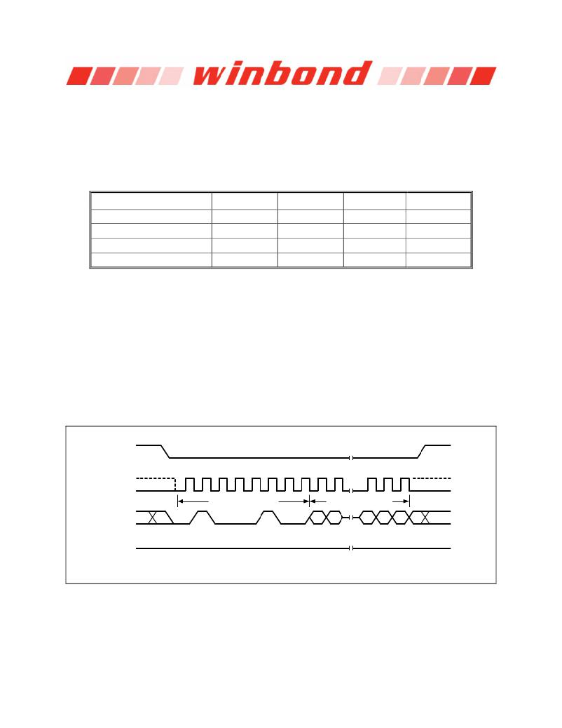
�The� Erase� Security� Register� instruction� sequence� is� shown� in� Figure� 34.� The� /CS� pin� must� be� driven� high�
�after� the� eighth� bit� of� the� last� byte� has� been� latched.� If� this� is� not� done� the� instruction� will� not� be� executed.�
�After� /CS� is� driven� high,� the� self-timed� Erase� Security� Register� operation� will� commence� for� a� time�
�duration� of� t� SE� (See� AC� Characteristics).� While� the� Erase� Security� Register� cycle� is� in� progress,� the� Read�
�Status� Register� instruction� may� still� be� accessed� for� checking� the� status� of� the� BUSY� bit.� The� BUSY� bit� is�
�a� 1� during� the� erase� cycle� and� becomes� a� 0� when� the� cycle� is� finished� and� the� device� is� ready� to� accept�
�other� instructions� again.� After� the� Erase� Security� Register� cycle� has� finished� the� Write� Enable� Latch�
�(WEL)� bit� in� the� Status� Register� is� cleared� to� 0.� The� Security� Register� Lock� Bits� (LB3-0)� in� the� Status�
�Register-2� can� be� used� to� OTP� protect� the� security� registers.� Once� a� lock� bit� is� set� to� 1,� the� corresponding�
�security� register� will� be� permanently� locked,� Erase� Security� Register� instruction� to� that� register� will� be�
�ignored� (See� 11.1.9� for� detail� descriptions).�
�/CS�
�Mode� 3�
�0�
�1�
�2�
�3�
�4�
�5�
�6�
�7�
�8�
�9�
�29�
�30�
�31�
�Mode� 3�
�CLK�
�Mode� 0�
�Instruction� (44h)�
�24-Bit� Address�
�Mode� 0�
�DI�
�(IO� 0� )�
�DO�
�High� Impedance�
�23�
�*�
�22�
�2�
�1�
�0�
�(IO� 1� )�
�*� =� MSB�
�Figure� 34.� Erase� Security� Registers� Instruction� (SPI� Mode� only)�
�Publication� Release� Date:� September� 06,� 2012�
�-� 61� -�
�Revision� F�
�发布紧急采购,3分钟左右您将得到回复。
相关PDF资料
W25Q16VSFIG
IC FLASH 16MBIT 80MHZ 16SOIC
W25Q32BVZPIG
IC SPI FLASH 32MBIT 8WSON
W25Q32DWZEIG
IC FLASH SPI 32MBIT 8WSON
W25Q40BWSSIG
IC FLASH SPI 4MBIT 8SOIC
W25Q40BWZPIG
IC FLASH SPI 4MBIT 8WSON
W25Q64BVSFIG
IC SPI FLASH 64MBIT 16SOIC
W25Q64CVZEIG
IC SPI FLASH 64MBIT 8WSON
W25Q64DWZEIG
IC FLASH SPI 64MBIT 8WSON
相关代理商/技术参数
W25Q16DWSFIP
制造商:WINBOND 制造商全称:Winbond 功能描述:1.8V 16M-BIT SERIAL FLASH MEMORY WITH DUAL/QUAD SPI & QPI
W25Q16DWSNIG
制造商:WINBOND 制造商全称:Winbond 功能描述:1.8V 16M-BIT SERIAL FLASH MEMORY WITH DUAL/QUAD SPI & QPI
W25Q16DWSNIP
制造商:WINBOND 制造商全称:Winbond 功能描述:1.8V 16M-BIT SERIAL FLASH MEMORY WITH DUAL/QUAD SPI & QPI
W25Q16DWSSIG
功能描述:IC FLASH SPI 16MBIT 8SOIC RoHS:是 类别:集成电路 (IC) >> 存储器 系列:SpiFlash® 标准包装:2,500 系列:- 格式 - 存储器:EEPROMs - 串行 存储器类型:EEPROM 存储容量:1K (128 x 8) 速度:100kHz 接口:UNI/O?(单线) 电源电压:1.8 V ~ 5.5 V 工作温度:-40°C ~ 85°C 封装/外壳:8-TSSOP,8-MSOP(0.118",3.00mm 宽) 供应商设备封装:8-MSOP 包装:带卷 (TR)
W25Q16DWSSIP
制造商:WINBOND 制造商全称:Winbond 功能描述:1.8V 16M-BIT SERIAL FLASH MEMORY WITH DUAL/QUAD SPI & QPI
W25Q16DWZPIG
制造商:Winbond Electronics Corp 功能描述:IC FLASH 16MBIT 104MHZ 8WSON
W25Q16DWZPIP
制造商:WINBOND 制造商全称:Winbond 功能描述:1.8V 16M-BIT SERIAL FLASH MEMORY WITH DUAL/QUAD SPI & QPI
W25Q16V
制造商:WINBOND 制造商全称:Winbond 功能描述:16M-BIT SERIAL FLASH MEMORY WITH DUAL AND QUAD SPI